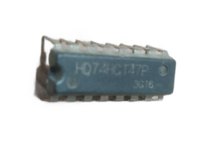

IC 7411 – Triple 3-Input NAND Gate (Pack of 2)
14 in stock
The IC 7411 is a quad 3-input NAND gate, part of the 7400 series TTL logic family. It contains four independent NAND gates, each with three inputs. This IC is used to perform logical NAND operations in digital circuits, making it suitable for creating complex logic functions and processing multiple input signals efficiently.
₹45.84 ₹94.40 (Incl. GST)
14 in stock
IC 7411 – Triple 3-Input NAND Gate (Pack of 2)
Overview
The IC 7411 – Triple 3-Input NAND Gate is a logic integrated circuit that contains three independent 3-input NAND gates. NAND gates are fundamental building blocks in digital electronics, and the IC 7411 is designed to provide efficient logic operations with three inputs per gate.
Features
- Triple 3-Input NAND Gates: Contains three separate NAND gates within one package, each with three inputs.
- TTL Compatible: Works with TTL (Transistor-Transistor Logic) logic levels, making it suitable for digital circuits.
- High Noise Margin: Provides a robust performance with a high noise margin for reliable logic operations.
- Low Power Consumption: Designed to operate efficiently with minimal power usage.
- Wide Operating Voltage Range: Can operate over a broad range of supply voltages for versatile applications.
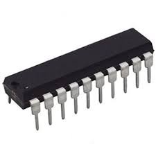
Pin Configuration
The IC 7411 is commonly available in an 14-pin Dual In-line Package (DIP) with the following pin configuration:
- Pin 1: Input (A1) – The first input of the first NAND gate.
- Pin 2: Input (B1) – The second input of the first NAND gate.
- Pin 3: Input (C1) – The third input of the first NAND gate.
- Pin 4: Output (Y1) – The output of the first NAND gate.
- Pin 5: Input (A2) – The first input of the second NAND gate.
- Pin 6: Input (B2) – The second input of the second NAND gate.
- Pin 7: Input (C2) – The third input of the second NAND gate.
- Pin 8: Output (Y2) – The output of the second NAND gate.
- Pin 9: Input (A3) – The first input of the third NAND gate.
- Pin 10: Input (B3) – The second input of the third NAND gate.
- Pin 11: Input (C3) – The third input of the third NAND gate.
- Pin 12: Output (Y3) – The output of the third NAND gate.
- Pin 13: Ground (GND) – Connects to the ground of the power supply.
- Pin 14: Supply Voltage (Vcc) – Positive supply voltage.
(Note: Pinout can vary slightly depending on the package type and manufacturer.)
Working Principle
- NAND Gate Operation: Each NAND gate in the IC 7411 performs a NAND operation, which is the complement of the AND operation. The output is LOW only when all inputs are HIGH; otherwise, the output is HIGH.
- Logic Expression: The output YY of a 3-input NAND gate can be expressed as Y=(A⋅B⋅C)‾Y = \overline{(A \cdot B \cdot C)}, where AA, BB, and CC are the inputs, and ⋅\cdot denotes the AND operation, while the overline denotes NOT.
- TTL Compatibility: The IC is compatible with TTL logic levels, which means it can interface with other TTL logic devices in digital circuits.
Applications
- Digital Logic Circuits: Used as a fundamental building block in various digital logic circuits.
- Data Processing: Useful in data processing and manipulation tasks within digital systems.
- Signal Conditioning: Can be used to condition or invert logic signals in digital applications.
- Arithmetic Logic Units (ALUs): Integral in constructing arithmetic and logic units within microprocessors.
Example Circuit
- Basic NAND Gate: Connect three inputs to pins 1, 2, and 3. The output will be available at pin 4. When all three inputs are HIGH, the output will be LOW; otherwise, it will be HIGH.
Advantages
- Multiple Gates in One Package: Provides three independent NAND gates in a single IC, saving space and reducing component count.
- Robust Performance: High noise margin and TTL compatibility ensure reliable operation.
- Versatile Applications: Suitable for a wide range of digital logic applications.
Conclusion
The IC 7411 is a versatile and essential component in digital electronics, offering three independent 3-input NAND gates within a single package. Its robustness, TTL compatibility, and ability to perform basic logic operations make it a valuable tool for constructing and managing digital circuits. Whether used in logic operations, signal conditioning, or data processing, the IC 7411 provides reliable and efficient performance.
Related products
-
74XX Series IC's
IC 74147 – BCD to Decimal Priority Encoder (Pack of 2)
The IC 74147 is a BCD to 7-segment priority encoder, part of the 7400 series TTL logic family. It converts a binary-coded decimal (BCD) input into a 7-segment display format while encoding the highest-priority input line active. This IC is used for numeric displays and encoding tasks, simplifying the process of converting BCD inputs into a displayable format.
SKU: ic-74147 -
74XX Series IC's
IC 74374 – Octal D-Type Flip-Flop with 3-State Outputs (Pack of 2)
The IC 74374 is an octal D-type flip-flop with 3-state outputs, part of the 7400 series TTL logic family. It includes eight independent D flip-flops, each with a data input (D), clock input (CLK), and output enable (OE) control. The 3-state outputs allow for flexible data bus interfacing and buffering in digital circuits, making it suitable for data storage, transfer, and manipulation applications.
SKU: ic-74374 -
74XX Series IC's
IC 74245 – Octal Bus Transceiver (Pack of 2)
The IC 74245 is an octal bidirectional buffer/driver with 3-state outputs, part of the 7400 series TTL logic family. It includes eight buffers/drivers, each with bidirectional data lines and control inputs for enabling or disabling the output. This IC is used for data bus interfacing and signal buffering, allowing for bidirectional data transfer and providing flexibility in digital circuit designs.
SKU: ic-74245 -
74XX Series IC's
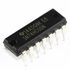
IC 7400 – Quad NAND Gate (Pack of 2)
The IC 7400 is a quad 2-input NAND gate, part of the 7400 series TTL logic family. It contains four independent NAND gates, each with two inputs. This IC is widely used in digital circuits for implementing NAND logic functions, enabling the creation of complex logic operations and signal processing in electronic systems.
SKU: ic-7400