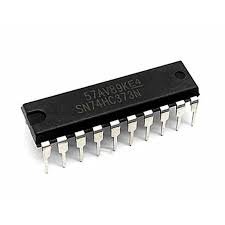
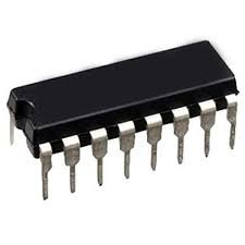
IC 74595 – 8-Bit Serial-in/Parallel-out Shift Register with 3-State Outputs (Pack of 2)
9 in stock
The IC 74595 is an 8-bit serial-in/parallel-out shift register with an output latch, part of the 7400 series TTL logic family. It allows for serial data input and parallel data output, making it useful for expanding the number of output pins on a microcontroller or for data storage and transfer in digital systems. It includes a latch to hold the output data, providing reliable data handling in various applications.
₹45.84 ₹94.40 (Incl. GST)
9 in stock
IC 74595 – 8-Bit Serial-in/Parallel-out Shift Register with 3-State Outputs (Pack of 2)
Overview
The IC 74595 is an 8-bit serial-in/parallel-out shift register with 3-state outputs, designed to handle both serial and parallel data operations. It is ideal for use in data storage, data transfer, and digital display applications where parallel output is needed from serial input.
Features
- 8-Bit Shift Register: Contains an 8-bit shift register for data storage and shifting.
- Serial-in/Parallel-out: Allows data to be entered serially and read out in parallel.
- 3-State Outputs: Provides high-impedance (3-state) outputs, enabling multiple devices to be connected to a common bus.
- Clocked Operation: Operates on clocked data input, capturing data on the clock edges.
- Synchronous Operation: Data is shifted in and out synchronously with the clock signal.
Pin Configuration
The IC 74595 is typically available in a 16-pin Dual In-line Package (DIP) format. The pinout is as follows:
- Pin 1: Q0 (Parallel Output 0)
- Pin 2: Q1 (Parallel Output 1)
- Pin 3: Q2 (Parallel Output 2)
- Pin 4: Q3 (Parallel Output 3)
- Pin 5: Q4 (Parallel Output 4)
- Pin 6: Q5 (Parallel Output 5)
- Pin 7: Q6 (Parallel Output 6)
- Pin 8: Q7 (Parallel Output 7)
- Pin 9: Vcc (Positive Supply Voltage)
- Pin 10: GND (Ground)
- Pin 11: SER (Serial Data Input)
- Pin 12: RCLK (Register Clock)
- Pin 13: SRCLK (Shift Register Clock)
- Pin 14: OE (Output Enable)
- Pin 15: SH/LD (Shift/Load Control)
- Pin 16: MR (Master Reset)
Working Principle
The IC 74595 operates as follows:
- Serial Data Input: Data is serially shifted into the shift register through the SER (Serial Data Input) pin, synchronized with the SRCLK (Shift Register Clock) signal.
- Parallel Data Output: The data in the shift register can be read out in parallel from the Q0 to Q7 pins.
- Shift/Load Control: The SH/LD pin controls whether the data is shifted into the register (shift mode) or loaded in parallel (load mode).
- Clock Signals: SRCLK controls the shifting of data, while RCLK controls the latching of parallel data outputs.
- Output Enable: The OE (Output Enable) pin controls whether the outputs are active or high-impedance.
- Reset: The MR (Master Reset) pin asynchronously clears all registers to zero.
Applications
- Data Storage: Stores and transfers data in digital systems, especially when parallel data needs to be accessed from a serial input.
- Display Drivers: Drives LED or LCD displays by converting serial data into parallel data for display elements.
- Data Conversion: Converts serial data streams into parallel data for processing and vice versa.
- Shift Registers: Acts as a shift register for various digital logic applications, including counters and data handling systems.
Example Circuit
- Display Controller: Use the IC to control a 7-segment display by serially loading data and outputting it in parallel to the display segments.
- Data Transfer: Implement the IC to transfer data serially from one part of a system and output it in parallel to another part.
Advantages
- 3-State Outputs: Allows connection to a shared data bus without interference from other devices.
- Synchronous Operation: Ensures reliable data transfer synchronized with clock signals.
- Versatile Data Handling: Provides both serial input and parallel output capabilities for flexible data management.
- Reset and Control: Includes features for master reset and control of shift/load operations.
Conclusion
The IC 74595 is a versatile and powerful 8-bit shift register that enables efficient serial-to-parallel data conversion and parallel data handling. Its 3-state outputs, synchronous operation, and shift/load control make it suitable for a wide range of digital applications, including data storage, display driving, and data conversion tasks. With its robust design and versatile features, the IC 74595 is a valuable component in modern digital systems.
IC 4085 – 8-Bit Serial-In/Parallel-Out Shift Register with 3-State Outputs (Pack of 2)


