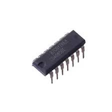
IC 4085 – 8-Bit Serial-In/Parallel-Out Shift Register with 3-State Outputs (Pack of 2)
25 in stock
The IC 4085 is a 4-bit binary up/down counter with a binary-coded decimal (BCD) output, part of the 4000 series CMOS logic family. It features a 4-bit counter that can count both up and down, and includes a carry-out feature for cascading multiple counters. It’s used in various digital applications, such as counting and frequency division, providing accurate and versatile counting capabilities.
₹45.84 ₹94.40 (Incl. GST)
25 in stock
IC 4085 – 8-Bit Serial-In/Parallel-Out Shift Register with 3-State Outputs (Pack of 2)
Overview
The IC 4085 – 8-Bit Serial-In/Parallel-Out Shift Register is a CMOS integrated circuit designed as an 8-bit serial-in/parallel-out shift register with three-state outputs. It is used for serial-to-parallel data conversion, allowing data to be shifted in serially and then output in parallel form.
Features
- Type: 8-bit shift register with serial input and parallel output.
- Serial Data Input: Allows for serial data to be shifted into the register.
- Parallel Outputs: Eight parallel outputs provide the data after shifting.
- 3-State Outputs: Outputs can be in high, low, or high-impedance state, which is useful for bus systems.
- Clock Input: Data is shifted on the clock’s rising edge.
- Power Supply: Typically operates between 3V to 15V.
- Package Type: IC 4085 – 8-Bit Serial-In/Parallel-Out Shift Register is Available in various packages, including DIP (Dual In-line Package), SOP (Small Outline Package), and others.
Pin Configuration
- Pin 1: Serial Data Input (DS).
- Pin 2: Shift Clock Input (SH_CP).
- Pin 3: Storage Clock Input (ST_CP).
- Pin 4: Output Enable (OE).
- Pin 5: Q0 (Parallel Output 0).
- Pin 6: Q1 (Parallel Output 1).
- Pin 7: Q2 (Parallel Output 2).
- Pin 8: Q3 (Parallel Output 3).
- Pin 9: Q4 (Parallel Output 4).
- Pin 10: Q5 (Parallel Output 5).
- Pin 11: Q6 (Parallel Output 6).
- Pin 12: Q7 (Parallel Output 7).
- Pin 13: Vcc (Power Supply).
- Pin 14: Ground (GND).
Applications
- Data Conversion: Used for converting serial data into parallel data for further processing or display.
- Bus Systems: The three-state outputs are useful for connecting multiple devices on a bus, allowing for proper data sharing and communication.
- LED Displays: Commonly used in driving LED displays, where data needs to be shifted and displayed in parallel.
- Peripheral Expansion: Suitable for expanding output lines in digital systems to control multiple peripherals.
Working Principle
The IC 4085 shifts data into the 8-bit register on each clock pulse applied to the shift clock input. The serial data is shifted in bit-by-bit, and once all bits are in the register, a pulse on the storage clock input latches the data into the parallel outputs. The output enable pin controls whether the outputs are active or in a high-impedance state.
Advantages
- Versatility: Provides a practical solution for serial-to-parallel data conversion and output expansion.
- Three-State Outputs: Allows for flexible data handling and integration into bus systems.
- Low Power Consumption: CMOS technology ensures efficient power usage.
The IC 4085 is a valuable component for applications requiring the conversion of serial data to parallel form, offering reliable performance and flexibility in various digital and electronic circuits.


