No products in the cart.
40XX Series IC's
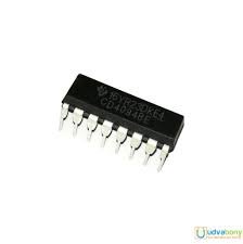
IC 4094 – 8-Bit Shift Register with Output Latches
Availability:
15 in stock
The IC 4094 is an 8-bit shift register with parallel output, part of the 4000 series CMOS logic family. It includes a serial-in, parallel-out configuration, allowing data to be shifted in serially and then accessed in parallel. This IC is commonly used for data storage, manipulation, and interfacing in digital circuits, offering flexibility for various applications.
₹31.86 ₹35.40 (Inc. GST)
15 in stock
IC 4094 – 8-Bit Shift Register with Output Latches
Overview
The IC 4094 – 8-Bit Shift Register with Output Latches is a CMOS (Complementary Metal-Oxide-Semiconductor) integrated circuit that functions as an 8-bit shift register with output latches. It is used for serial-to-parallel conversion, which allows for the shifting of data in serial form and then outputting it in parallel form.
Features
- Type: 8-bit shift register with output latches.
- Data Input: Serial input for shifting data into the register.
- Parallel Output: Eight parallel outputs that provide the shifted data.
- Clock: Shifts data on the clock’s rising edge.
- Output Latches: Each output has a latch that holds the data when the register is not shifting.
- Power Supply: Typically operates between 3V to 15V.
- Package Type: IC 4094 – 8-Bit Shift Register with Output Latches Available in various packages, including DIP (Dual In-line Package), SOP (Small Outline Package), and others.
Pin Configuration
- Pin 1: Serial Data Input (DS).
- Pin 2: Shift Clock Input (SH_CP).
- Pin 3: Storage Clock Input (ST_CP).
- Pin 4: Output Enable (OE).
- Pin 5: Q0 (Parallel Output 0).
- Pin 6: Q1 (Parallel Output 1).
- Pin 7: Q2 (Parallel Output 2).
- Pin 8: Q3 (Parallel Output 3).
- Pin 9: Q4 (Parallel Output 4).
- Pin 10: Q5 (Parallel Output 5).
- Pin 11: Q6 (Parallel Output 6).
- Pin 12: Q7 (Parallel Output 7).
- Pin 13: Vcc (Power Supply).
- Pin 14: Ground (GND).
Applications
- Data Storage: Used to temporarily store data in digital circuits.
- Data Shifting: Ideal for applications requiring serial-to-parallel data conversion.
- LED Displays: Commonly used in driving 7-segment or LED displays where data needs to be shifted and displayed in parallel.
- Peripheral Expansion: Useful in expanding the number of output lines for controlling multiple peripherals.
Working Principle
The IC 4094 – 8-Bit Shift Register with Output Latches operates by receiving serial data and shifting it into the 8-bit register on each clock pulse applied to the shift clock input. The data is then latched into the output latches when a pulse is applied to the storage clock input, making it available on the parallel outputs. The output enable pin controls whether the outputs are active or in a high-impedance state.
Advantages
- Versatility: Can be used in a variety of applications requiring data shifting and storage.
- Ease of Use: Simplifies the process of converting serial data to parallel data.
- Low Power Consumption: CMOS technology ensures efficient power usage.
The IC 4094 – 8-Bit Shift Register with Output Latches is a valuable component for digital circuits that need to convert serial data into parallel form, providing a practical solution for data management and peripheral control in various electronic applications.


There are no reviews yet.